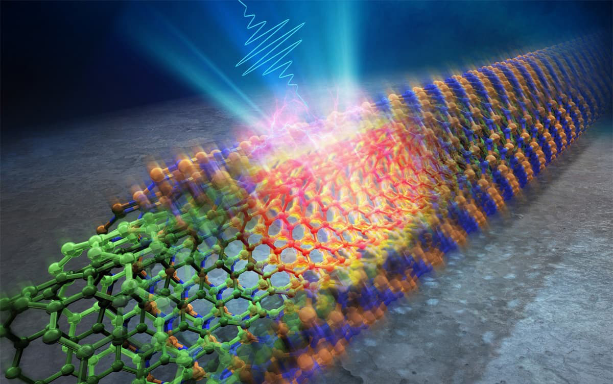
Recent studies within the Dynacom framework have shown that low-dimensional materials, composed of atomically thick layered tubes, display new properties. Researchers created structures by wrapping carbon nanotubes (CNTs) in boron nitride nanotubes (BNNTs) and used ultrafast optical spectroscopy and time-resolved electron diffraction to monitor electron and atomic motion. They discovered that electrons could transfer between layers, converting their energy into thermal energy rapidly. This finding reveals a new physical phenomenon at the interface of these materials, suggesting potential applications in ultrafast optical devices and electron manipulation. Image of a nested structure of carbon nanotubes enveloped in boron nitride nanotubes under photoexcitation. Credit: University of Tsukuba
Research shows rapid electron and thermal transfers in layered materials, aiding optical tech.
Researchers have identified new characteristics of layered low-dimensional materials that enable rapid transfers of electrons and thermal energy, pointing to potential improvements in ultrafast optical technologies and various other applications.
In a collaborative work in the Dynacom framework (French Japanese Laboratory), recent studies have highlighted that materials composed of layered tubes, which are atomically thick and classified as low-dimensional materials, exhibit new properties. Although the static properties of these structures, such as electrical conduction, are well documented, their dynamic properties, including electron transfer between layers and atomic motion triggered by light exposure, have received less attention.
In this study, researchers constructed nested cylindrical structures by wrapping carbon nanotubes (CNTs) in boron nitride nanotubes. They then examined the motion of electrons and atoms induced by ultrashort light pulses on a one-dimensional (1D) material. Electron motion was monitored using broadband ultrafast optical spectroscopy, which captures instantaneous changes in molecular and electronic structures due to light irradiation with a precision of ten trillionths of a second (10−13 s). Atomic motion was observed through ultrafast time-resolved electron diffraction, which similarly achieved monitoring of structural dynamics with ten-trillionth-of-a-second accuracy.
Discovery of New Physical Phenomena
The study revealed that when different types of low-dimensional materials are layered, a pathway or channel forms, allowing electrons to escape from specific subparts of the material. Additionally, it was found that electrons excited in the CNTs by light exposure could transfer into the BNNTs via these electronic channels, where their energy is rapidly converted into thermal energy, facilitating extremely fast thermal conversion.
This research has uncovered a new physical phenomenon at the interface between two dissimilar materials, offering not only ultrafast thermal energy transport but also potential applications in the development of ultrafast optical devices and the rapid manipulation of electrons and holes generated by light.
Reference: “Photoinduced dynamics during electronic transfer from narrow to wide bandgap layers in one-dimensional heterostructured materials” by Yuri Saida, Thomas Gauthier, Hiroo Suzuki, Satoshi Ohmura, Ryo Shikata, Yui Iwasaki, Godai Noyama, Misaki Kishibuchi, Yuichiro Tanaka, Wataru Yajima, Nicolas Godin, Gaël Privault, Tomoharu Tokunaga, Shota Ono, Shin-ya Koshihara, Kenji Tsuruta, Yasuhiko Hayashi, Roman Bertoni and Masaki Hada, 30 May 2024, Nature Communications.
DOI: 10.1038/s41467-024-48880-3
This work was supported by JSPS Kakenhi Grants-in-Aid [Nos. JP18H05208 (S.K.), JP22KK0225 (M.H.) and JP23H01101 (M.H.)] and the Japan Science Technology Agent (JST) FOREST Program [No. JPMJFR211V (M.H.)]. R.B. acknowledges Agence Nationale de la Recherche (ANR) for funding undergrant, ANR-21-CE30-0011-01 CRITICLAS.