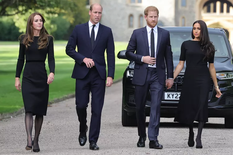
Prince William Set to Remove Meghan Markle’s HRH Title As Royals Prepare For Transition
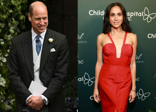
Prince William is reportedly planning to strip Meghan Markle and Prince Harry of their HRH titles once he ascends to the British throne, according to a royal insider. The source told The Daily Beast that while King Charles III might tolerate the situation, William is determined to take action against what he sees as a violation of royal protocol.
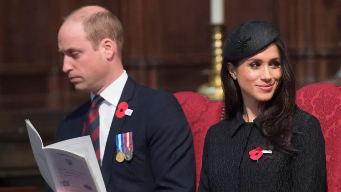
The tension stems from Markle’s continued use of the HRH title in the promotion of her lifestyle brand, As Ever, which includes products like a pricey jam. The insider claims that William views this as an exploitation of royal status for commercial gain, something he finds unacceptable. “He loathes and despises Harry and Meghan with every bone in his body,” the source stated, adding that William believes they have betrayed everything the monarchy stands for.
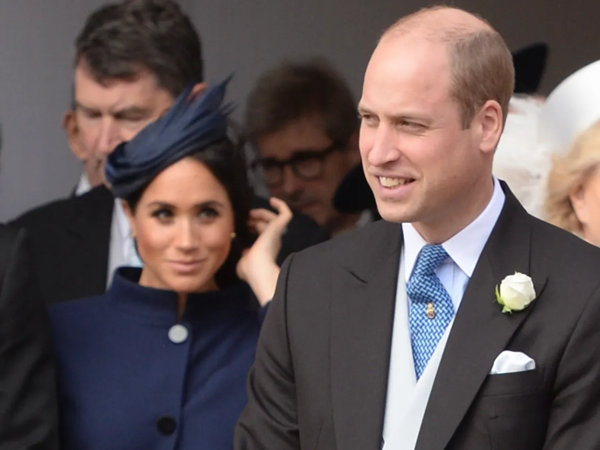
Markle’s use of the HRH title was reportedly in violation of an agreement made with the late Queen Elizabeth II, which stipulated that the Duke and Duchess of Sussex would no longer use their royal titles for commercial purposes following their exit from royal duties. This came to light after Markle signed a gift basket with the HRH title while promoting homemade strawberry sauce on a podcast. The note accompanying the basket read, “With the Compliments of HRH The Duchess of Sussex,” raising concerns about her adherence to the agreement.
A friend of Prince William’s insisted that Markle’s continued use of the HRH title exposes King Charles’ perceived weakness. The friend stated, “Charles has completely lost control,” and that Markle knows he won’t take action. “There is no way King William will stand for this,” the source added. “The titles will simply be removed when he is king.”
However, a representative for Markle denied that she was in violation of the agreement, claiming that the gift was personal and not used for commercial purposes. “Harry and Meghan retain their HRH titles; however, by agreement, they do not use them for commercial purposes,” the source explained. “While they do not publicly use ‘HRH,’ this was a personal gift, and their titles remain.”
A former courtier refuted Markle’s defense, describing it as “rubbish.” The former royal aide emphasized that the terms of the Sussexes’ departure from royal duties were clear in that they agreed not to use their HRH titles in any capacity. This claim is backed by an official statement from the couple’s exit agreement, which explicitly stated they would not use their HRH titles as non-working royals.
Harry and Meghan, who stepped back from their senior royal roles in 2020, now live in California with their two children, Prince Archie and Princess Lilibet. Since their move, Markle has launched her Netflix series With Love, Meghan and debuted her lifestyle brand, As Ever, which includes several popular products.
Despite facing criticism for their commercial ventures, Markle’s Netflix show has been renewed for a second season, and her brand continues to grow in popularity. It remains to be seen how Prince William’s plans for the Sussexes’ titles will unfold once he ascends the throne.
Source link